

Convincing Features

Assignment Type
Subject
Uploaded by Malaysia Assignment Help
Date
This assignment covers:
Ability to evaluate the CMOS transistor characteristics. Conduct investigations of complex problems using research-based knowledge (WK8) and research methods including design of experiments, analysis, interpretation of data, and synthesis of the information to provide valid conclusions.
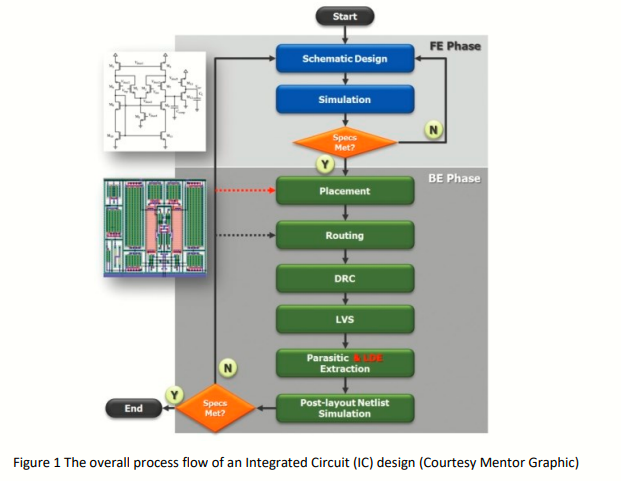
Figure 1 shows the overall process flow of an Integrated Circuit (IC) design.
SULIT
The operation begins with Front End Phase by creating the transistor-level schematic design based on the design specifications, before proceeding with the simulation step. In this simulation step, the test benches are required to verify the functionality of the design.
Next, the operation continues with Back End Phase by designing the layout based on the schematic design. Several steps are involved in this layout design phase such as Pre-layout design which includes Placement and Routing steps. Layout designers can always try different device placements and examine
the impact of any specific configuration of device placement on the original specification. Then, the process continues with DRC (Design Rule Check) and LVS (Layout Versus Schematic) steps. A successful DRC ensures that the layout conforms to the rules designed for faultless fabrication, while the successful LVS ensures that the layout connectivity of the physical design matches the schematic design.
Students in NMJ216043 was exposed to all the design process mentioned earlier. However, to achieve a successful post-layout design that meets all the specifications, important tasks like parasitic extraction is required. Students should be aware that the behavior of the layout design is extremely sensitive to the layout-induced parasitics such as inductance, resistance, and capacitance. Parasitics not only influence the layout performance but often render it non-functional. Hence, it is essential to consider the effect of parasitics in the design process. In conclusion, the major purpose of parasitic extraction is to create an accurate layout of a circuit, so that the simulations can emulate the actual circuit responses.